

|
The VFO currently used in the receiver is a Vacker circuit shown below. To improve stability, a "Huff and Puff" stabilizer is used with magnetic coupling. |
|
This circuit is from "Meet the Vacker: The Simple, Stable VFO You've Been Looking For", By Mark L. Meyer, QEX, July 1997, Page 8.
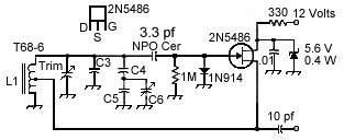
One of the more interesting statements in the article was "Vacker developed a circuit decades ago that is simple and provides uncommon short-and-long-term stability without the use of fancy phase-locked loops or other control circuitry." (Page 8) The circuit, with the values shown, operates between 4.570 and 4.646 MHz. To change the values for the frequency you want, multiply the values by the ratio of your desired frequency to 4.570 MHz. "For example, if you wish to have a frequency of 3.500 MHz, you multiply C1-C7 and L1 by 1.3 (4.57/3.5) Frequencies higher than 4.75 will result in a multiplier value less than one." (Page 8) Q1 is a MPF102 or a 2N5486. One of the interesting things I discovered was that my 2N4416's would not work in this circuit. My suggestion is that if the circuit does not oscillate, try different FETs that are in the junk box. I like the 2N5486 over the MPF102 because the 2N5486 has proven to be more frequency stable than the MPF102. C8, C9 and C10 are used as compensation capacitors for the variable-capacitor diodes and have a negative coefficient factor. If you can't find these, use the emitter-base of a 2N3904 as a temperature compensator for the varactors. Shown below is a modified circuit showing the 2N3904 circuit.
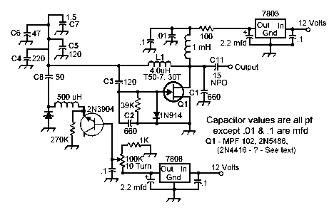 C1 and C2 should use parallel capacitors to aid stability (circulating currents are shared) and be NPO, C0G, or polystyrene capacitors. C8 serves a dual purpose. If it is a negative coefficient capacitor, it helps compensate the tuning diode, but it also isolates the DC tuning voltage from the rest of the circuit. The tuning diode can be of any value or type. Usually the MV21** series are used or the MV1662 recommended in the article. Also, high voltage rectifiers work well as tuning diodes. The article shows a very simple printed circuit board layout, but using 'dead bug style' has worked great and is recommended. |
|
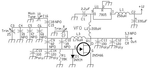
The important capacitors are the poly caps (C11, C12, C13, and C14). Other values should be split in a combination to give 220pf and be poly to provide the best stability. The C3 trim cap is used to set the VFO frequency to 10.455 MHz, along with C7. The reason for the large value of C3 was the receiver was first set up for 40 and 20 meters, and C3 was used to set the frequency to 10.455 MHz (20 meters) or 10.545 MHz (40 Meters). C3 is a panel mount capacitor that was originally used as an antenna trimmer in the HQ-140-X. Approximately 17pf of C3 is used to set the frequency to 10.455 MHz. C15 is used to restrict the tuning range to 100 kHz. It value can be changed to effect the bandwidth to the desired range. The sharp filters preclude the reception of SSB, so 100 to 150 kHz was all the bandwidth that was needed. The reason for the multitude of NPO capacitors was to help stability, so circulating RF currents would be shared to help stability. Different values can be used as long as they add up to the same values in the schematic. C9 and C10 should be the best NPOs that can be obtained. They are critical for good stability. Any drift in these caps has a huge effect on VFO frequency. Again, different values can be used, as long as the total capacitance is the same. C16 is one section of the original main tuning capacitor of the HQ-140-X. The VFO is placed in the metal box with the main tuning capacitor. This box, along with the cabinet of the HQ-140-X, provides a very stable temperature environment for the VFO. L3 is 18 turns #20 wire on a T68-6 toroid cord. A ceramic coil form can be used, or even a self supporting open wire coil. A T80-6 or T68-6 provide better stability than a T50-6 core and are easier to wind. If a "Huff and Puff" stabilizer is used, wire size should be reduced to #24, to help the relay used with the stabilizer have the maximum range possible. See the Electoluminescent Receiver section on the Frequency Stabilizer for more information. L2 can be any value close to 200uH. But it should have good thermal properties to help with stability. I wound my own RF choke on a FT50A-75 core with 7 turns, which is a value a lot lower than 200uH, but a large core helps stability. With an FT50-43 core, wind as many turns with #24 or #22 wire that will fit. A molded choke cannot be used for L2, because if one of the trim caps is shorted to ground while adjusting the VFO, it will blow a molded choke (welding the wires together - losing its choking ability) and then blow the 2N5486. Both the RF choke (L2) and the toroid (L3) should be covered with wax from a household candle to keep air from reaching the cores. Metallic substances absorb temperature changes faster than the poly caps and you will lose the balance of the positive and negative temperatue coefficients of the different parts. The wax also provides excellent mechanical stability. L1 and C2 can be any value. They help with the isolation of RF currents from the VFO to the 12 Volts bus. C1 (2.2mfd) is a standard value used at the output of three terminal voltage regulators to keep the regulator from oscillating. |
|
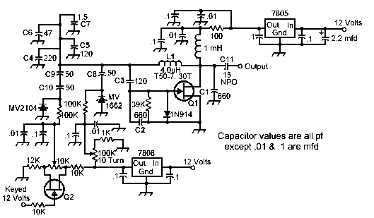
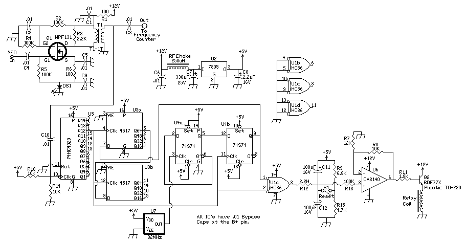
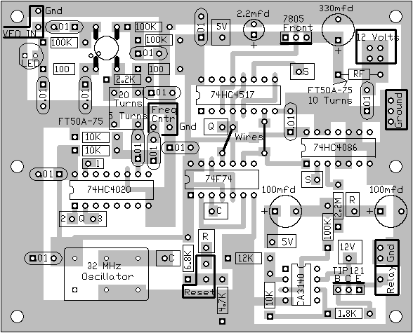
The credit for this circuit goes to Hans Summers, who developed the circuit after my suggestion that magnetic coupling would work with a frequency stabilizer. It uses a shift register (74HC4517) as a memory for the stabilizer and provides excellent stability. At the present time, it is in the experimental stage and is being used with this receiver to evaluate its performance. So far, it has worked very well. One problem that has surfaced at times is that the output transistor (TIP121 - used as the relay driver) can get warm and start to drift. This causes the stabilizer to lose lock and will quit working. A transistor with a plastic case, also in a TO-220 (see schematic) package, is being used that shows better resistance to warming up than one with a metal heat sink. The output transistor has to be grossly overrated for the current supplied to the relay to prevent the transistor from warming up and causing an increase in current to the relay. Relays with coil resistance higher than 200 ohms work best. A coil resistance of 120 ohms or similar draw a lot of current and it is harder to keep the transistor cool. A Power MOSFET would not have this problem of increasing current with heat, but I have not been able to get a power MOSFET to work. I'm sure that one could be made to work, but so far my efforts have not hit on the magic solution. For those that don't want to build this circuit from scratch, I offer a stabilizer kit using a circuit developed by Klaas Spaarjaren, PA0KSB, the inventor of the "Huff and Puff", for $20.00. See the Electroluminescent Reciever section on the Frequency Stabilizer. This circuit has been used for many years and is time proven. The performance between this circuit and the one above is hardly noticable. |
Other Good Quality VFO CircuitsWhat follows here are descriptions of three different VFO circuits. The FET, a transistor low-noise design, and the NE602 used as a VFO. I have built and used them all except the transistor low-noise design. My favorite is the NE602, which I use in almost all my equipment where I need a 10 to 14MHz VFO. I have the FET at 10MHz in two receivers and it works great. I plan to experiment with the transistor low-noise design extensively, as it appears to be a really neat design. Just choose the one you have parts for, or try a new design you haven't tried yet. They all work great. A CMOS buffer can follow a VFO for a square wave signal into a diode mixer. "A CMOS Buffer For VFO's" will convince you to take the trouble for a square wave.
FET VFO Oscillators
 This circuit comes from the Progressive Communications Receiver that is in most of the recent ARRL Handbooks and the article "A Progressive Communications Receiver", by Wes Hayward and John Lawson, QST, November 1981, Page 11. C4 and C5 are adjusted in value so that C6, of almost any value, can be used in this VFO. The formulas for calculating the proper values are on page 21 in the November 1981 of QST. Working without the formulas, C4 in series with C6 will effectively lower C6's value and shorten its range. The parallel capacitor C5 will also shorten the range of C6, and lower the low end frequency of the VFO. Use C3 to make major changes in the frequency of the VFO. The values for this receiver are the following:
L1 - 20 Turns, Tap - 5 Turns from ground end The values given above are for a VFO that will work with the 3.457 MHz crystal filter: 40 meters - 10.547MHz and up, 20 meters - 10.453MHz and up. This circuit can be used at frequencies between 2.5 to 10 MHz.
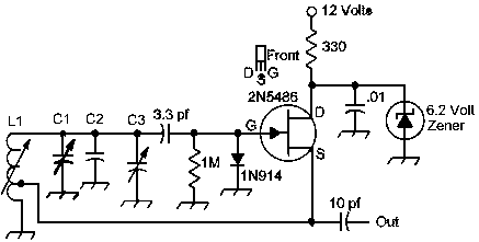 The above circuit is like the one at the top, simplified somewhat. C1 is the trimmer capacitor and C3 is the main tuning. If you have a small capacitor that can be used as the main tuning, this circuit is easy to set to the proper frequency by C1, C2 and the toroid winding. This VFO is probably the most stable FET circuit out there, but I have found that the active device you use can make a big difference in the stability of the VFO. With the MOSFET (Gates 1 & 2 tied together), the VFO drifted considerably on warm up and was very sensitive to temperature variations. When a 2N5486 was used, there was very little warm-up drift and stability during minor temperature variations was acceptable. More information is available for this circuit in the ARRL 2000 Handbook, page 14.19-20. For an 11.1MHz VFO, the values are the following:
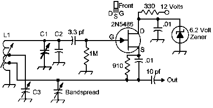
L1 - B&W #3041 10 Turns (#22 wire, 5/8 dia, 24 tpi) Tap 2 1/2 Turns from Ground End An interesting variation on the circuit in the 2002 ARRL Handbook was the elimination of the diode off the gate of the FET, and the inclusion of a 910 ohm resistor in parallel with a .01 capacitor in the source lead. Bandspread and bandset capacitors were tied to taps on L1 to give the required ranges. The complete circuit was credited to KA2WEU, KA7EXM, W7ZOI, and W7EL. A similar circuit was used in "The Ugly Weekender" and the "Optimized QRP Transceiver". See diagram below for the updated circuit.
VFO Transistor Buffer Circuit
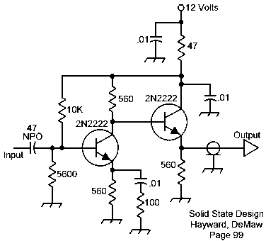 In the first design of the receiver, this buffer was used with an FET VFO oscillator followed by a filter and a 2N5109 amplifier.
The K7HFD Low-Noise Oscillator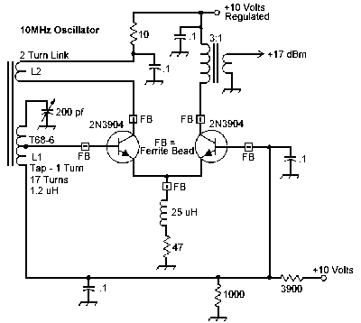 This circuit appears in the ARRL 2000 Handbook, Page 14.18, and in Solid State Design for the Radio Amateur, by Wes Hayward & Doug DeMaw, Page 126. No buffer is necessary with this VFO. There is enough drive to go directly to a diode mixer. Operating description is quoted from Solid State Design, Page 126: "The voltage from the resonator, which is applied to the base, causes the collector current to change. This changing collector current is coupled back into the resonator through a link which is arranged to yield the proper phase for positive feedback. The maximum peak current that can be supplied to the link is the current standing in the transistor pair. This is defined by the emitter resistor and the inductor, which has the effect of making the current appear to originate from a constant current source. With the peak collector current well defined, the voltage across the tank is also well defined and limited." From the ARRL 2000 Handbook, Page 14.19: "With an output of +17 dBm, this is a power oscillator, running with a large dc input power, so appreciable heating results that can cause temperature-induced drift. The circuit's high-power operation is a deliberate ploy to create a high signal-to-noise ratio by having as high a signal power as possible." "The amplitude must be controlled by the drive current limit. The voltage on L2 must never allow the collector of the transistor driving it to go into saturation, if this happens, the transistor presents a very low impedance to L2 and badly loads the tank, wrecking the Q and the noise performance. The circuit can be checked to verify the margin from saturation by probing the hot end of L2 and the emitter with an oscilloscope. Another, less obvious , test is to vary the power-supply voltage and monitor the output power, but if the supply is low enough to allow saturation, the output power will change significantly." "...the results of a phase-noise test made using a spectrum analyzer with a crystal filter as a preselector are given. Ten kilohertz out from the carrier in a 3-kHz measurement bandwidth, the noise was over 120 dB below the carrier level. This translates into better than -120 - 10 log (3000), which equals -154.8 dBc/Hz, SSB. At this offset, -140 dBc is usually considered to be excellent. This is state-of-the art performance by today's standards - in a 1977 publication." There is more information in the 1999 and 2000 ARRL Handbook on this circuit on Page 14.19. Circuit operation is more detailed in the Handbook than in the Solid State Design book.
NE602 VFO OscillatorIt's my opinion that the NE602 may have been overlooked as one of the most stable VFO oscillators around. In the Signetics application note "Applying the Oscillator of the NE602 in Low Power Mixer Applications", the NE602 is described as a chip with three subsystems, a Gilbert cell mixer, a buffered emitter follower oscillator, and RF current and voltage regulation. Please note the third system - "RF Current and Voltage Regulation". The bias is temperature compensated for RF and current variations. This means that the NE602 does not drift or contribute to the drift in any way. After using an NE602, you will be surprised at how much a factor the active device drift plays a part in VFO stability. I have found the NE602 oscillator to be rock solid from the instant it is turned on. The VFO circuit is very easy to design for any frequency (see NE602 Front End) and uses fewer parts than the FET VFO. The downside is that the NE602 is more expensive than a single FET, and is more susceptible to frequencies floating on the 12 Volts line, which requires careful bypassing and maybe some shielding. A 7805 voltage regulator does a great job of isolating the NE602 from the 12 Volts line. The combination of a 7805 voltage regulator and the NE602 makes a very stable VFO with a minimum of effort. The extra $5 is worth the expense. To use the NE602 as an oscillator only , I quote from the article "NE602 Primer", by Joseph J. Carr, Elector Electronics USA, January 1992, Page 25 (picture is Fig. 10 on page 25):
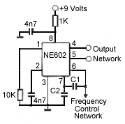 "The NE602 is usually thought to be a receiver or frequency converter, but it can also be used as an oscillator or signal generator. Normally, the LO signal and the RF signal are suppressed in the output. Figure 10 shows a generic circuit that will allow the LO signal to appear at the output (no RF or IF signal appears). In this circuit, one RF input (pin 2) is bypassed to ground for RF, while the other input (pin 1) is grounded for d.c. through a 10k resistance." The following circuit is the one I developed. The VFO runs at either 3MHz or 4MHz and the appropriate crystal is beat against the VFO to get the frequency I want. It is very stable and easy to build. |
|
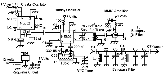
If you're not going to be mixing, you can eliminate the crystal oscillator and use a 10K resistor between Pin 1 and ground. The bandpass filter is not needed either, since there are no mixing products. For VFO's in the 10MHz to 20MHz range, this mixing scheme works fantastic. The crystal oscillator works with almost any crystal. Some 3 to 4MHz crystals needed the 33 pf capacitor to be raised to 56 pf or so. The 220pf cap at pin 7 of the second NE602 should be a poly cap to provide the best stability. It compensates for the temperature coefficient of the T80-6 toroid. A T68-6 or T50-6 toroid can also be used. The higher the crystal frequency (10MHz and up), the lower the output from the crystal oscillator, and the lower the output of the frequency you want. Lower crystal frequencies (2MHz to 10MHz) yield higher output, but more trouble with mixing products. The bandpass filter helps tremendously in removing unwanted mixing products, and cleans up the signal beautifully. Don't accidentally use a lowpass filter here from a QRP or other transmitter project, as these filters won't remove the lower frequency products. Bandpass filters from receiver projects work great. The bandpass filter shown above is from the "Progressive Communication Receiver". For other frequencies, check out the Solid State Design book, Page 238. See tables below for values.
The output from the VFO NE602 is very low. The MMIC amplifier lifts the signal level enough to pass through the bandpass filter in good shape. Any MMIC will work here. There are some MMIC's in the catalogs with the part number 1651 that work great. The MAR-* series of MMIC's work fine, also. Be careful, some MMIC's feed the power through the output lead. Double check yours to make sure you wire it correctly. The 1651 is wired as shown in the schematic. Two stages of amplification are needed. A good combination is the Variable MOSFET VFO amplifier followed by the 2N5109 (w/resistive pad) into a diode mixer. |
Send E-Mail || Amateur Radio Receivers || Super Receiver || Super Receiver Circuit Details